- To be a global leader in overmolding protection industry.
Whole area processing logic with image processing technology
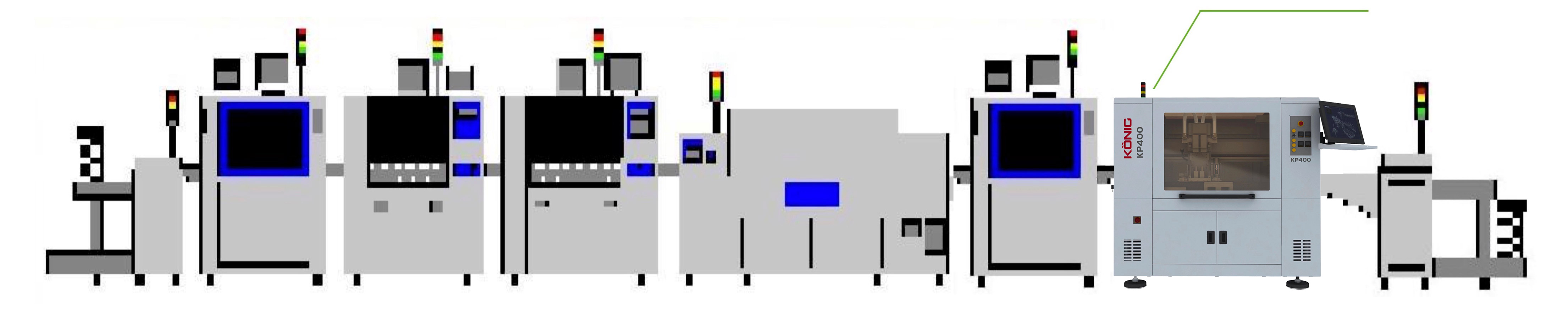
Process Flow

No need masking tape
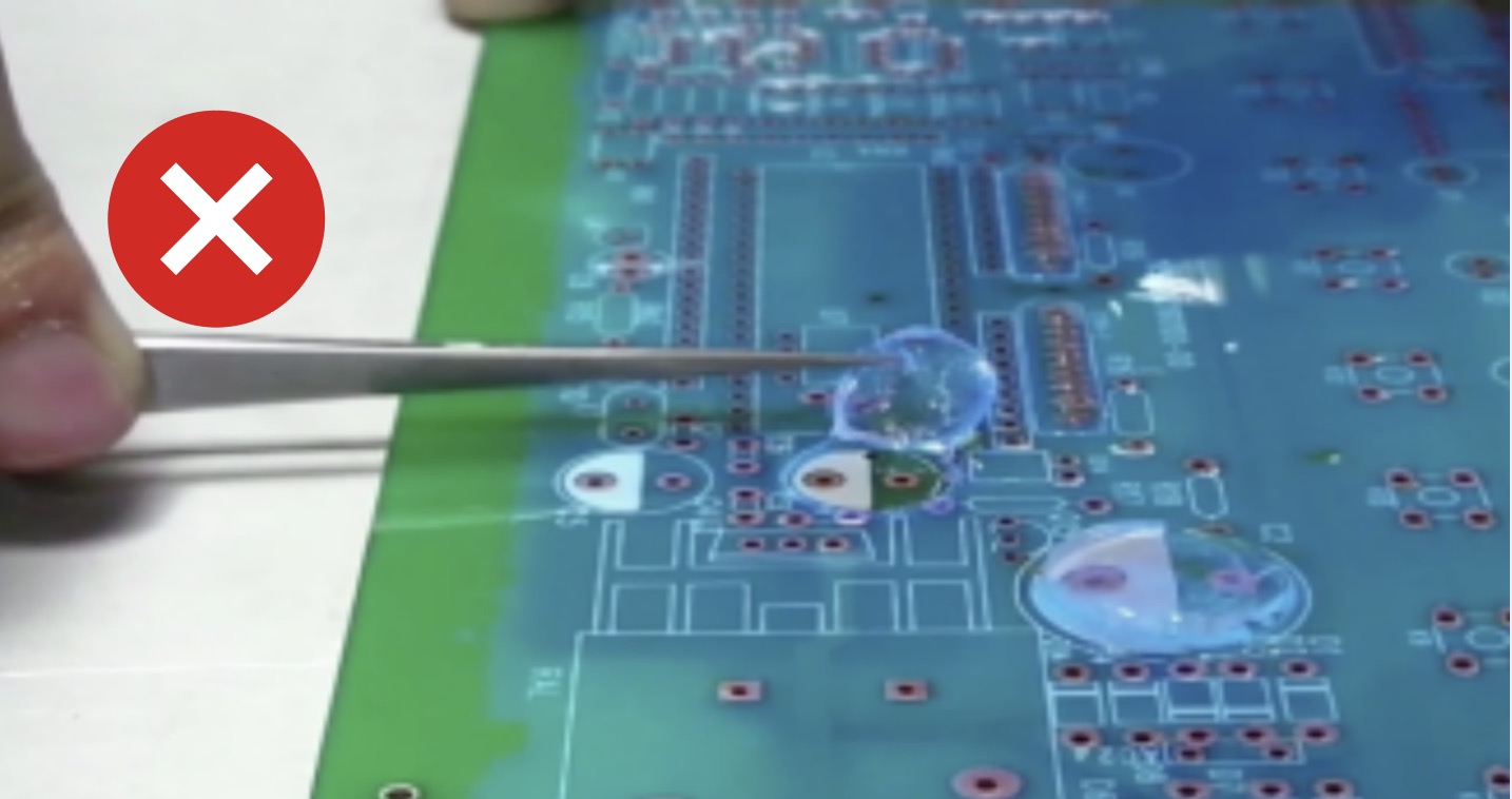
No need masking glue
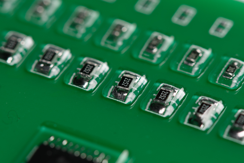
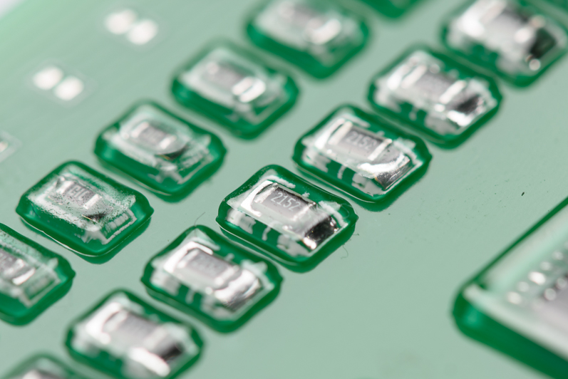
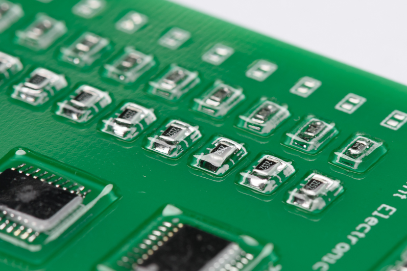
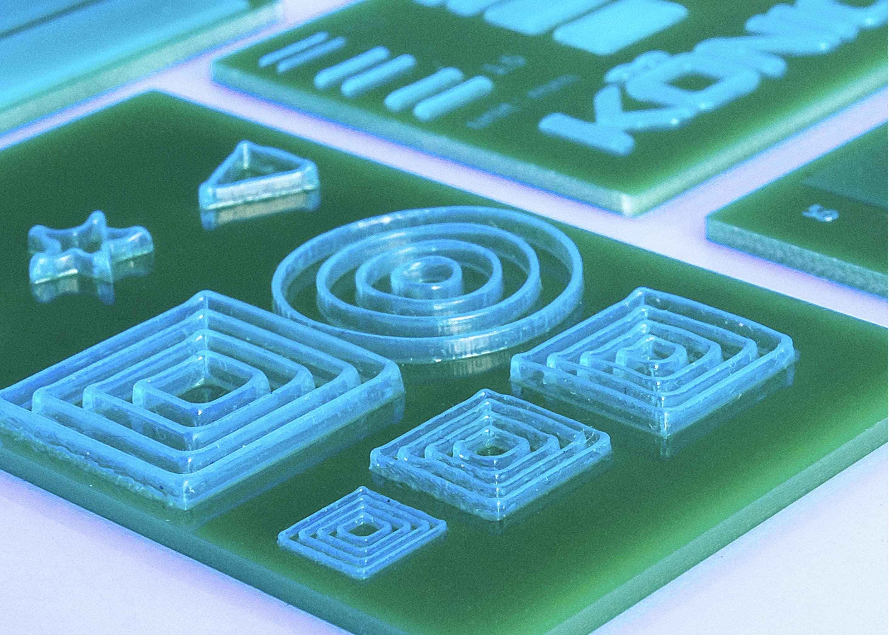
Dispensing, Coating
implemented on one device, realizing different protection levels
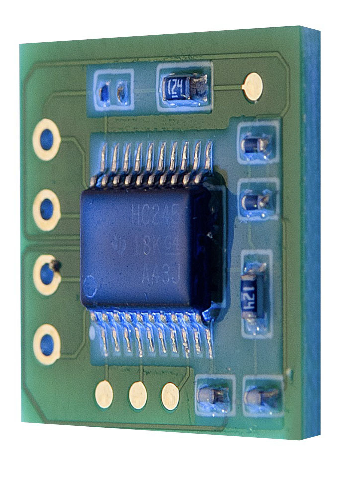
Thin layer coating
general protection

Thick layer coating
high-grade protection
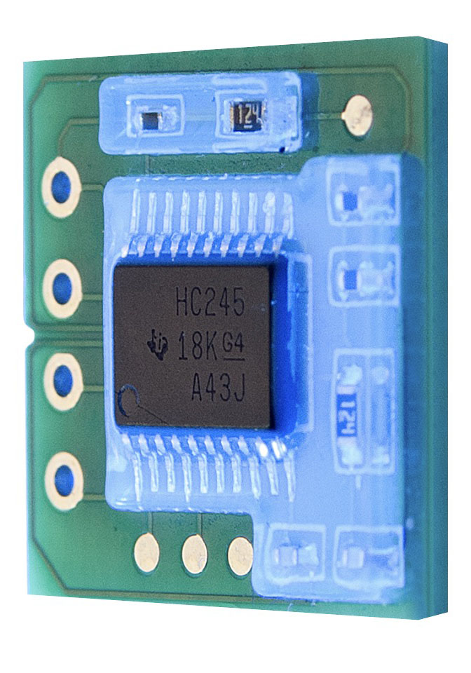
Fence + filling
with same UV glue
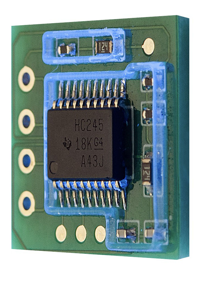
Separate fence
fill with any glue
Actions speak louder than words
"The production process that used to take a few minutes, now only takes a few seconds."
The protection area is 10*10mm
glue can be saved at least 1/3
Auxiliary process
no need to masking, no need wait for curing
60 μm thickness is required
accuracy and thickness can be guaranteed
Environmental
no solvent volatilization and no need special protection
Production efficiency
only need 10s, efficiency increased dozens of times
Time is money, especially for the busy SMT production line. Although PCBA protection is a later process, the efficiency and effectiveness directly affect the delivery cycle and yield of PCBA. This is especially true for mass and multi variety production lines. PCBA needs to be coated for many times in order to meet the protection requirements. If you want to get a thicker coating, the conformal coating needs to be obtained by applying two thinner coatings, and the second layer must be applied after the first layer is fully cured. It takes time to cure completely. The digital packaging process is different. UV-Led is cured with follow-up while spraying, and the second layer can be sprayed immediately with controllable thickness.
PCBA packaging protection is completed by a more accurate and simplified process, which does not need to wait for curing and occupy the curing site. This is especially true for a large number of circuit boards that need protection. "Some of these batches may occupy the workshop for several days, so it is very important to save a few minutes per board."
Choosing a reliable process is also an improvement to the quality of the product.
01
High precision nozzle driven by image software
02
Mark point recognition system
03
UV-Led follow curing device
04
Ink cartridge circulation system
05
Temperature control system
06
High reliable 4-axis motion platform
Freely control the glue thickness to achieve higher precision packaging protection
After the UV glue is sprayed, the UV-Led is follow up to solidified automatically,
and the 2nd layer can be sprayed immediately.
The thickness of the single layer is 25 microns,
and the stacking thickness of the layers is controllable.
The process is safe and environment-friendly without waste water and waste gas

No water pollution
No solvent evaporation

No need special protection

Low energy consumption

Green material

Environment friendly